
Semiconductor Etch Equipment Market Overview :
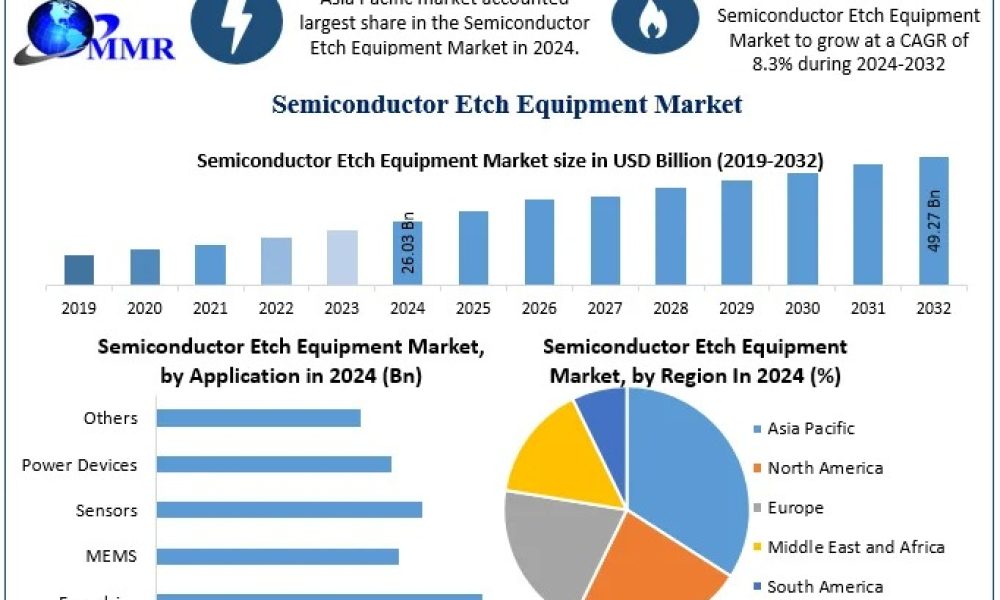
Semiconductor Etch Equipment Market, valued at USD 26.03 billion in 2024, is expected to surge to USD 49.27 billion by 2032, registering a robust CAGR of 8.3%. The market’s growth is propelled by cutting-edge innovation, booming semiconductor manufacturing, and strategic investments in Asia Pacific—especially across China, South Korea, Taiwan, and Japan.
Key Highlights & Insights
Market Size & Growth: The market is projected to expand from USD 26.03 billion (2024) to USD 49.27 billion (2032), growing at a CAGR of 8.3%.
Dominating Region: Asia Pacific holds the largest share, leveraging its leadership in global foundries, rising investments in semiconductor manufacturing, and government incentives, notably China’s ambitious semiconductor stimulus totaling over $143 billion from 2022 onward.
Leading Segment: Conductor etch equipment tops the segment due to its crucial role in sculpting the minute electrically activated structures of next-gen microchips; precision, selectivity, and advanced plasma/dry etching methods are pivotal.
Key Driver: The rapid proliferation of electronics in automotive, consumer, and industrial applications—combined with massive government support for local semiconductor sectors and global supply chain shifts—continues to fuel demand for advanced etch tools.
Recent Developments
March 2024: Lam Research launched the world’s first production-oriented Pulsed Laser Deposition (PLD) system, advancing MEMS and RF filter manufacturing with high-performance materials.
April 2023: Hitachi High-Tech broke ground on a new automated, digitalized etch system production facility in Yamaguchi, Japan, to double output and meet surging demand from global chipmakers.
2022 & Beyond: AlixLab unveiled its Atomic Layer Etch Pitch Splitting (APS) method, radically reducing process steps and resource intensity for chip fabrication—streamlining next-gen semiconductor production.
Governments in China and Japan rolled out billion-dollar stimulus packages, subsidies, and partnerships to accelerate domestic fab and equipment production, fortifying Asia’s dominance.
For full access to the data, request a sample report now :https://www.maximizemarketresearch.com/request-sample/78567/
Market Dynamics
Growth Drivers:
Increasing wafer and chip production for consumer, automotive, datacenter, and IoT markets.
Continuous advances in semiconductor fabrication, requiring ultra-precision etching, higher throughput, and reduced defects.
Strong government programs (SPECS in India, local incentives in China and Japan) encourage expansion, R&D, and global competitiveness.
Challenges:
Trade uncertainties, especially U.S.-China tensions and evolving global regulations, disrupt supply chains and market confidence.
Raw material shortages and supply chain delays exert pressure on equipment manufacturers and fab operators.
Evolving design complexities and the need for specialized, skilled engineering talent present ongoing hurdles.
Regional Analysis
Asia Pacific: Dominant region with Taiwan, Korea, China, and Japan serving as major foundry and equipment centers. India’s proactive policies boost new fabs and investments, transforming the region’s competitive landscape.
North America: Key leadership in equipment innovation (Lam Research, Applied Materials, KLA Corp.), with notable growth in fab investments (Micron in India) and technology partnerships.
Europe: Strong position in specialty equipment and etch solutions, with expansion in production automation and sustainable practices.
Rest of World: Growing investments in Brazil, Southeast Asia, and the Middle East supporting diversification and local chipmaking capabilities.
Product Segmentation
By Type: Wet etch equipment, dry etch equipment.
By Process: Dielectric etch, conductor etch (largest share), other processes innovating around selectivity and control.
By Application: Semiconductor foundries (largest segment), MEMS, sensors, power devices, and specialty chip production.
Key Trends
Atomic layer, high-selectivity, and pitch-splitting technologies enable ever-smaller chip geometries and higher packing densities.
Integration of automation, process control, and AI-driven inspection improves yield and throughput.
Regional manufacturing shifts and vertical integration among foundries and equipment suppliers.
Emphasis on sustainable practices, energy-efficient operations, and reduction of environmental impact in semiconductor fabrication.
Quote
Asia Pacific’s rapid ascent in semiconductor manufacturing, backed by next-generation etch equipment and robust government support, is rewriting the global supply chain landscape. As innovation accelerates, precision etching technologies will remain at the core of the digital economy’s transformation.
With relentless chip demand and transformative investments across Asia, the semiconductor etch equipment market will remain the backbone of technological progress, enabling foundational advances in computing, communications, and automotive innovation worldwide.