
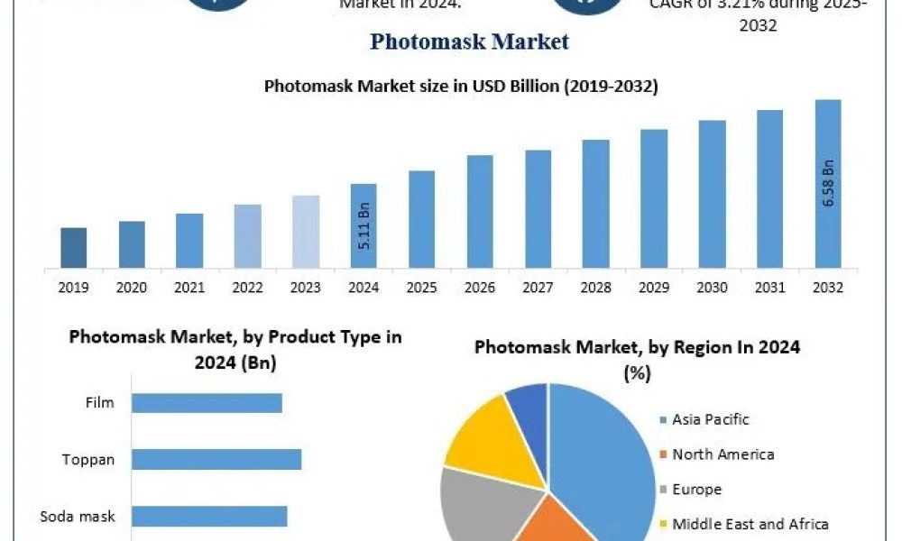
Photomask Market is undergoing significant expansion, propelled by the ever-growing needs of the semiconductor, electronics, flat panel display, PCB, and MEMS industries. Valued at around USD 5.11 billion in 2024, the market is projected to rise to nearly USD 6.58 billion by 2032 with a steady CAGR of 3.21%. Growth is especially concentrated in Asia Pacific—where countries such as Taiwan, South Korea, China, and Japan lead in semiconductor fabrication and display manufacturing—backed by a complex value chain and substantial investments in modern lithography technologies.
Market Overview & Dynamics
Photomasks are crucial stencil-like plates used in photolithography during the manufacture of integrated circuits, printed circuit boards, displays, and MEMS devices. Consisting of substrates like quartz, glass, or film coated with opaque chrome, photomasks efficiently transfer intricate micro-patterns onto semiconductor wafers, enabling large-scale production of microelectronic devices. The industry benefits from trends in digital transformation, 5G deployment, IoT adoption, AI growth, and an increasing proliferation of consumer electronics—all heightening the global demand for advanced semiconductors and, consequently, photomasks.
Key drivers supporting this market’s momentum include:
Rising Semiconductor Content: As chip demand accelerates for smartphones, automotive applications, AI accelerators, advanced memory, and 5G, the need for high-resolution, defect-free photomasks becomes paramount.
Growth of High-End Lithography: Adoption of extreme ultraviolet (EUV) lithography and high-NA (numerical aperture) EUV is spurring demand for next-generation masks—reflective, multilayered, and precision-written for sub-5nm production nodes.
Consumer Electronics and Display Evolution: Increasing popularity of OLED, AMOLED, and high-resolution LCDs requires stringent display mask technologies—supporting television, smartphone, and wearable device markets.
Regional Insights
Asia Pacific is the unchallenged dominant region, accounting for over 44% of the global photomask market revenue in 2024. Semiconductor powerhouses like Taiwan and South Korea have the most advanced chip foundries, while China’s rising manufacturing output solidifies the region’s market presence. Investments in local fabrication plants, such as China’s aggressive foundry buildout and continued expansion in Japan and Taiwan, reinforce APAC’s leadership. North America, while smaller in absolute share, is a fast-growing region thanks to the CHIPS Act, which supports domestic semiconductor manufacturing and new mask production capacity. Europe is making concerted efforts to localize chip supply but is still catching up in manufacturing capacity and scale.
For full access to the data, request a sample report now :https://www.maximizemarketresearch.com/request-sample/35762/
Market Segmentation & Applications
The photomask market is segmented by:
Product Type: Quartz masks, soda masks, toppan films, binary masks, phase-shift masks (PSM), and advanced EUV masks.
Application: Semiconductor (leading), flat panel display, circuit board, touch industry, MEMS/optical devices.
Mask Shop Type: Captive mask (in-house for large IC manufacturers) and merchant mask (for foundries and IDMs).
Semiconductor photomasks account for about 30% of total demand, reflecting the ongoing push for miniaturization and increasing lithographic complexity in the chip industry. Advanced packaging, chiplets, and silicon photonics drive new requirements for reticle and large-area masks, especially for AI, automotive, and high-bandwidth applications.
Market Trends & Technological Innovations
EUV and High-NA EUV Lithography: The evolution to high-NA EUV (especially in Korea and Taiwan) and movement to sub-3nm nodes is giving rise to photomasks with extreme accuracy, multilayer reflective stacks, and advanced defect mitigation. The EUV segment is forecast to grow above the industry average, as these masks are critical for enabling cutting-edge logic and memory ICs.
Inspection & Repair with AI: The rise of AI-enabled mask inspection and defect repair tools improves test time, reduces error rates, and supports increasingly fine geometries in both merchant and captive mask shops.
Supply Chain Localization: With disruptions from COVID-19 and geopolitical concerns, major geographies are incentivizing local mask production and investing in high-purity quartz and advanced mask writers/inspectors to reduce overseas reliance.
Sustainability & Cost Efficiency: Competitive pricing, increased mask recycling, and investments in repair instead of replacement are lowering costs and ecological impact. However, high development costs remain a key challenge, especially for EUV masks.
Competitive Landscape & Recent Developments
The market is highly consolidated, with prominent players including Hoya, Dai Nippon, SK-Electronics, Toppan Photomasks, Photronics, LG Innotek, and Taiwan Mask.
Recent developments include:
Installation of Mycronic SLX1 laser writers in European facilities, boosting regional capabilities and echoing global investment trends.
Strategic mergers and capacity expansions in mask shops and mask-making equipment, offsetting quartz substrate shortages and supply chain vulnerabilities.
Merchant mask shops are rising, particularly as the U.S. and EU inject incentives for local mask manufacturing to support new fab construction.
Challenges & Outlook
Production complexity, input material shortages (notably high-purity quartz), and the high capital cost of advanced mask writing/inspection are limiting factors for market expansion. Despite these challenges, robust downstream demand and essential roles in advanced technology nodes will continue to fuel steady photomask market growth.
Conclusion & Outlook
The photomask market stands as a vital enabler of semiconductor scaling, display innovation, and electronics miniaturization. With Asia Pacific at the forefront—and North America/EU rapidly increasing investments—the industry is set for incremental growth anchored by technology shifts, regional policy support, and relentless end-use demand. As manufacturing sophistication and next-generation lithography proliferate, photomask manufacturers will remain central to the digital economy’s future.