
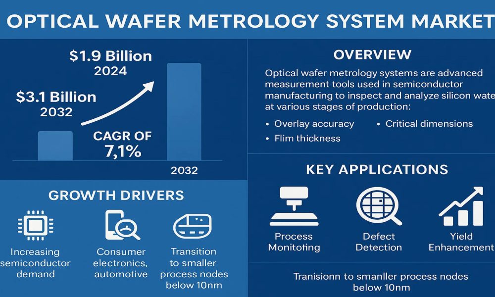
Optical Wafer Metrology System Market size was valued at US$ 1.9 billion in 2024 and is projected to reach US$ 3.1 billion by 2032, at a CAGR of 7.1% during the forecast period 2025-2032.
Optical wafer metrology systems are advanced measurement tools used in semiconductor manufacturing to inspect and analyze silicon wafers at various stages of production. These systems utilize high-precision optical technologies to measure critical parameters such as overlay accuracy, critical dimensions, and film thickness, ensuring quality control in chip fabrication. Key applications include process monitoring, defect detection, and yield enhancement.
The market growth is driven by increasing semiconductor demand across consumer electronics, automotive, and communication devices, coupled with the transition to smaller process nodes below 10nm. However, the market faces challenges from the high cost of advanced metrology systems and cyclical semiconductor industry fluctuations. Major players like ASML Holding NV and KLA Corporation continue to innovate, with recent developments including AI-powered defect classification and multi-beam measurement technologies to address emerging industry requirements.
Claim Your Free Sample Report-https://semiconductorinsight.com/download-sample-report/?product_id=107303
MARKET DYNAMICS
MARKET DRIVERS
Expanding Semiconductor Industry to Fuel Demand for Optical Wafer Metrology Systems
The global semiconductor industry continues its robust growth trajectory, directly driving demand for optical wafer metrology systems. With semiconductor manufacturers pushing the boundaries of miniaturization and chip complexity, the need for precise measurement and inspection tools has never been higher. The semiconductor market is projected to reach $1 trillion by 2030, creating significant opportunities for metrology equipment providers. Optical wafer metrology plays a crucial role in ensuring yield optimization and process control, particularly as chipmakers transition to smaller node technologies below 5nm where dimensional tolerances become increasingly stringent.
Advancements in 3D NAND and EUV Lithography Driving Technical Innovation
The evolution of 3D NAND flash memory technology and the adoption of extreme ultraviolet (EUV) lithography are creating new requirements for wafer metrology systems. As 3D NAND manufacturers stack more layers – with some products now exceeding 200 layers – traditional metrology approaches become insufficient. Optical wafer metrology systems capable of measuring deep trench profiles and complex 3D structures are seeing growing adoption. Similarly, EUV lithography’s introduction has created demand for metrology solutions that can characterize extremely fine features with sub-nanometer precision.
Moreover, the increasing complexity of advanced packaging technologies like chiplets and 3D ICs is further expanding the application scope for optical wafer metrology. These trends are prompting metrology system manufacturers to develop new measurement techniques and enhanced software algorithms to maintain measurement accuracy on next-generation semiconductor devices.
Recent Developments:
- Adoption of AI-driven metrology solutions – Major players are integrating AI and machine learning algorithms with optical wafer metrology systems to enhance defect detection accuracy and process optimization.
- Focus on advanced semiconductor nodes – Growing demand for sub-5nm and 3nm wafer inspection has driven innovation in high-resolution optical metrology tools.
- Integration with EUV lithography – Optical wafer metrology systems are increasingly designed to support extreme ultraviolet (EUV) lithography processes, which are crucial for next-generation chips.
- Shift toward 3D NAND and advanced packaging – Rising adoption of 3D NAND flash and heterogeneous integration has accelerated the need for more precise wafer surface metrology.
- Collaborations and partnerships – Companies like KLA, Hitachi High-Tech, and Nova are partnering with semiconductor fabs to co-develop tailored metrology solutions.
- Automation and Industry 4.0 integration – Automated, real-time wafer inspection systems are being implemented to increase throughput and reduce production costs.
- Sustainability initiatives – Equipment manufacturers are focusing on energy-efficient optical metrology systems to align with the semiconductor industry’s green manufacturing goals.
MARKET OPPORTUNITIES
Growing AI Implementation in Metrology Creating New Growth Avenues
The integration of artificial intelligence and machine learning into optical wafer metrology systems presents significant opportunities for market growth. AI-enhanced metrology can improve measurement accuracy, reduce false defect detection, and enable predictive maintenance capabilities. These smart systems can analyze vast amounts of measurement data to identify subtle process variations that might indicate emerging yield issues. As semiconductor manufacturers increasingly adopt Industry 4.0 practices, demand for intelligent metrology solutions is expected to grow substantially.
Expansion of Semiconductor Manufacturing Capacity Creating Installation Opportunities
Major semiconductor manufacturers worldwide are significantly expanding production capacity in response to global chip shortages and government initiatives to strengthen semiconductor supply chains. For instance, the CHIPS Act in the United States has allocated $52 billion to boost domestic semiconductor manufacturing, while similar initiatives exist in Europe and Asia. These capacity expansions will require substantial investments in metrology equipment, creating significant opportunities for optical wafer metrology system providers in both new and existing fabrication facilities.
Claim Your Free Sample Report-https://semiconductorinsight.com/download-sample-report/?product_id=107303
List of Key Optical Wafer Metrology System Companies Profiled
- ASML Holding NV (Netherlands)
- KLA Corporation (U.S.)
- Chroma ATE Inc. (Taiwan)
- Confovis GmbH (Germany)
- Onto Innovation Inc. (U.S.)
- Quality Vision International Inc. (U.S.)
- TZTEK Technology Co., Ltd. (China)
- QES Mechatronic Sdn Bhd (Malaysia)
Segment Analysis:
By Type
Fully Automatic Optical Wafer Metrology Systems Lead Due to High Precision in Semiconductor Manufacturing
The market is segmented based on type into:
- Fully Automatic Optical Wafer Metrology System
- Subtypes: In-line systems, stand-alone systems
- Semi-Automatic Optical Wafer Metrology System
By Application
Communication Devices Segment Dominates Driven by Rising Demand for 5G and IoT Chips
The market is segmented based on application into:
- Communication Devices
- Subtypes: RF components, network processors
- Consumer Electronics
- Car Parts
- Subtypes: ADAS components, vehicle control units
- Others
By Technology
Optical Scatterometry Gains Traction for Non-Destructive Wafer Measurements
The market is segmented based on technology into:
- Optical Scatterometry
- Ellipsometry
- Reflectometry
- Interferometry
By Measurement Type
Overlay Measurement Segment Shows Strong Growth for Process Control Applications
The market is segmented based on measurement type into:
- Overlay Measurement
- Critical Dimension Measurement
- Film Thickness Measurement
- Defect Inspection
Other Topic-Multi-Fiber Connector Market
CONTACT US:
City vista, 203A, Fountain Road, Ashoka Nagar, Kharadi, Pune, Maharashtra 411014
[+91 8087992013]