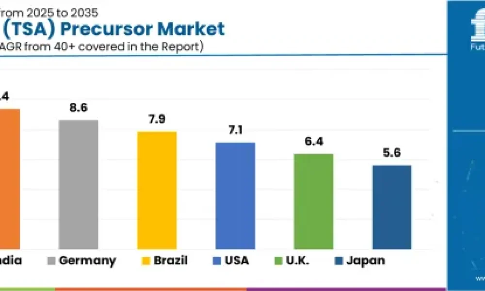
The global trisilylamine (TSA) precursor market is entering a high-growth decade, projected to surge from USD 26.1 million in 2025 to USD 53.7 million by 2035, according to the latest analysis from Future Market Insights (FMI). This expansion represents an impressive 105.7% total growth, a 7.5% CAGR, and a near 2.06X market increase during the forecast window.
This exceptional rise is powered by rapid advancements in semiconductor manufacturing, rising penetration of atomic layer deposition (ALD) technologies, and stringent purity requirements for next-generation logic and memory devices.
Strong Two-Phase Growth Outlook Through 2035
The market’s fastest expansion will occur between 2030 and 2035, adding USD 16.3 million, which accounts for 59.1% of the decade’s total growth. This phase will be dominated by:
- Scale-up of advanced semiconductor fabrication
- Integration of TSA-based ALD processes in 3D NAND and logic nodes
- Demand for ultra-high purity precursors to support atomic-scale thickness uniformity
- Specialized precursor formulations for emerging device geometries
Between 2020 and 2025, the market already gained significant traction as semiconductor fabs increasingly adopted TSA for silicon nitride deposition due to its superior thermal stability, decomposition behavior, and contamination-free properties—parameters essential for yield optimization.
Subscribe for Year-Round Insights → Stay ahead with quarterly and annual data updates: https://www.futuremarketinsights.com/reports/sample/rep-gb-26823
Quick Global Stats (FMI)
- Market Value 2025: USD 26.1 million
- Market Value 2035: USD 53.7 million
- CAGR (2025–2035): 7.5%
- Top Purity Grade: ≥99.9% (58% share)
- Fastest-Growing Markets: China, India, Germany
- Leading Applications: CVD (52%), ALD (fastest-rising)
Why the TSA Precursor Market Is Growing
- Advanced Node Semiconductor Requirements
Miniaturization and high-performance chip designs demand ultra-thin dielectric layers and immaculate film uniformity. TSA offers unmatched conformality and step coverage, making it critical for 3D memory, FinFET architectures, and advanced logic devices.
- Rise of ALD and High-Volume Deposition
ALD adoption is accelerating for its atom-by-atom precision. TSA’s stable vapor pressure, clean decomposition, and low impurity footprint have made it a preferred choice for high-purity nitride layers.
- Stringent Purity Standards
Semiconductor fabs worldwide increasingly require precursors with analytical certifications and impurity levels below critical device thresholds. TSA meets these specifications, especially at ≥99.9% purity, which dominates with 58% market share.
- Global Semiconductor Capacity Expansion
APAC’s fabrication boom, U.S. R&D resurgence, Europe’s precision chemical ecosystem, and Saudi Arabia’s strategic industrial diversification are collectively fueling precursor demand.
Segmental Insights
Purity Grade: ≥99.9% Leads with 58% Share
The ultra-high purity segment is the industry’s backbone owing to:
- Zero-defect film deposition
- Superior electrical properties
- Improved device reliability
- Advanced distillation and analytical processes that ensure consistent chemical signatures
This segment continues to benefit from innovation in handling systems, inert packaging, and contamination-free delivery modules.
Application: CVD Dominates with 52% Share
CVD remains the largest application due to:
- Its established use in silicon nitride deposition
- High thermal stability and controlled decomposition of TSA precursors
- Expansion of large-wafer manufacturing and multi-layer barrier film requirements
- Strong demand from advanced packaging and 3D integration
ALD, while smaller, is the fastest-accelerating sub-segment due to atomic-scale deposition requirements in advanced nodes.
Regional Market Outlook: APAC, Europe, USA & Saudi Arabia
Asia-Pacific: Global Growth Engine
China (10.1% CAGR) leads worldwide with aggressive expansion in DRAM, NAND, and logic chip manufacturing. Government-backed programs and large fabrication parks drive demand for ultra-high purity TSA.
India (9.4% CAGR) emerges as a high-potential market fueled by electronics manufacturing expansion, PLI incentives, and rising investments in advanced semiconductor materials infrastructure.
Japan and South Korea continue to adopt high-purity formulations for precision applications and advanced memory manufacturing.
Europe: Precision Manufacturing Stronghold
Germany (8.6% CAGR) anchors the region with its advanced chemical engineering capabilities and rigorous purity compliance.
The United Kingdom (6.4% CAGR) and France (16.4% regional share) are supported by strong materials science programs and semiconductor research clusters.
Europe’s market is set to rise from USD 7.1 million (2025) to USD 12.8 million (2035) at a 6.1% CAGR.
United States: Innovation-Driven Adoption
Growing at 7.1% CAGR, the U.S. market benefits from:
- Strong semiconductor R&D ecosystems
- Increased funding for next-generation node development
- Demands from advanced chip design and materials innovation
Saudi Arabia & GCC: Emerging Industrial Hub
Saudi Arabia’s advanced materials and electronics initiatives align with national diversification programs, boosting:
- Local semiconductor ecosystem development
- High-purity precursor adoption
- Fabrication and packaging infrastructure modernization
Saudi Arabia is becoming a notable future demand center for TSA in the Middle East.
Need tailored insights? Request report customization to match your specific business objectives: https://www.futuremarketinsights.com/customization-available/rep-gb-26823
Key Trends Shaping the Decade Ahead
- Automation & Process Monitoring: Real-time mass spectrometry, purity monitoring, and automated delivery systems enhance consistency.
- Next-Generation Purification Technologies: Ultra-clean distillation, inert storage, and sealed delivery modules achieve unprecedented purity levels.
- Specialized Formulations: Tailored precursor chemistries support emerging chip architectures and extreme scaling requirements.
- Regional Supply Chain Localization: APAC and GCC initiatives accelerate domestic TSA production and reduce import dependencies.
Competitive Landscape
According to FMI, the market is moderately consolidated, with manufacturers investing in:
- Advanced purification systems
- Ultra-high purity analytics
- Specialized packaging
- On-site technical support
Core market participants span multinational chemical suppliers and regional electronics material producers, leveraging high-purity capabilities and semiconductor-grade certifications.
About Future Market Insights (FMI)
Future Market Insights, Inc. (FMI) is an ESOMAR-certified, ISO 9001:2015 market research and consulting organization, trusted by Fortune 500 clients and global enterprises. With operations in the U.S., UK, India, and Dubai, FMI provides data-backed insights and strategic intelligence across 30+ industries and 1200 markets worldwide.
Why Choose FMI: Empowering Decisions that Drive Real-World Outcomes: https://www.futuremarketinsights.com/why-fmi