
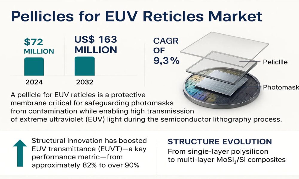
Pellicles for EUV Reticles Market was valued at 72 million in 2024 and is projected to reach US$ 163 million by 2032, at a CAGR of 9.3% during the forecast period.
A pellicle for EUV reticles is a protective membrane critical for safeguarding photomasks from contamination while enabling high transmission of extreme ultraviolet (EUV) light during the semiconductor lithography process. These components are essential for maintaining yield and precision in advanced chip manufacturing, particularly as node sizes shrink below 7nm. The structure of EUV pellicles has evolved significantly, transitioning from initial single-layer polysilicon designs to advanced multi-layer composites utilizing alternating molybdenum disilicide (MoSi₂) and silicon (Si) layers. This structural innovation has boosted EUV transmittance (EUVT)—a key performance metric—from approximately 82% to over 90%.
The market is experiencing robust growth driven by the escalating demand for advanced semiconductors, fueled largely by artificial intelligence (AI), high-performance computing, and the Internet of Things (IoT). The proliferation of EUV lithography systems, which now operate at power levels exceeding 500W, necessitates high-performance pellicles to protect reticles from thermal and particulate damage. Key industry players, including Mitsui Chemicals—which began mass sales in 2021 after licensing technology from ASML—are advancing next-generation carbon nanotube (CNT) pellicle technologies, with new production facilities expected by the end of 2025. Other notable contributors, such as S&S Tech and Canatu, are also developing high-transmittance and durable pellicle solutions to meet the stringent requirements of leading semiconductor manufacturers.
Receive Your Sample Report at No Cost- https://semiconductorinsight.com/download-sample-report/?product_id=117543
MARKET DYNAMICS
MARKET DRIVERS
Accelerated Adoption of EUV Lithography in Advanced Semiconductor Manufacturing to Drive Market Expansion
The global semiconductor industry’s relentless pursuit of miniaturization has created unprecedented demand for extreme ultraviolet lithography technology, which is the primary driver for EUV pellicle adoption. With over 80% of all sub-7nm semiconductor manufacturing now utilizing EUV lithography, the requirement for high-performance pellicles has become critical. The transition to multi-layer pellicle structures has significantly improved EUV transmittance rates from approximately 82% to over 90%, enabling more efficient chip production. Major semiconductor manufacturers have increased their EUV tool investments by approximately 40% year-over-year, with leading foundries operating more than 60 EUV systems globally. This substantial capital expenditure directly translates to increased pellicle consumption, as each EUV system requires multiple pellicles for different mask sets throughout the production process.
Rising Demand for High-Performance Computing and AI Chips to Boost Market Growth
The exponential growth in artificial intelligence applications and high-performance computing has created an insatiable demand for advanced semiconductor chips manufactured using EUV technology. The AI chip market, which relies heavily on EUV-produced components, is projected to grow at a compound annual growth rate exceeding 35% through 2030. This growth directly correlates with increased pellicle demand, as each EUV lithography process requires specialized pellicles to protect photomasks from contamination. The complexity of AI processors, featuring transistor counts exceeding 50 billion units per chip, necessitates multiple EUV patterning layers, further driving pellicle consumption. Additionally, the automotive industry’s shift toward autonomous driving systems has created new demand for advanced semiconductors, with electric vehicles containing approximately 3,000 chips per vehicle, many requiring EUV manufacturing processes.
Furthermore, the ongoing global semiconductor capacity expansion, particularly in leading semiconductor manufacturing regions, is expected to sustain market growth. Major semiconductor manufacturers have announced capacity expansion projects totaling over $200 billion in investments, with a significant portion allocated to EUV-capable facilities.
➤ For instance, leading semiconductor foundries have increased their EUV pellicle procurement by approximately 60% in the past two years to support their advanced node manufacturing capabilities.
The convergence of 5G deployment, IoT expansion, and cloud computing growth continues to drive semiconductor demand, ensuring sustained market growth for EUV pellicles throughout the forecast period.
Recent Developments in Pellicles for EUV Reticles Market
- Advanced Material Innovations
- Companies are developing pellicles using ultra-thin, high-transmittance materials to withstand extreme ultraviolet (EUV) radiation without degradation.
- New materials improve durability and reduce defects during the photolithography process, boosting semiconductor yield.
- Expansion of Manufacturing Capacity
- Leading manufacturers are expanding production facilities to meet the growing demand from semiconductor foundries, especially in regions with advanced chip production like Taiwan, South Korea, and the U.S.
- Strategic partnerships between pellicle manufacturers and EUV scanner companies are being formed to ensure timely supply.
- Enhanced Protective Capabilities
- Recent pellicles offer improved particle protection on EUV masks, reducing mask contamination and defects.
- Innovations include hydrophobic and anti-reflective coatings to further minimize potential lithography errors.
- Collaborations and Strategic Alliances
- Market leaders are collaborating with chipmakers to co-develop next-generation pellicles optimized for 5nm and 3nm process nodes.
- These alliances aim to streamline adoption of EUV lithography in high-volume manufacturing.
- Focus on Sustainability
- Companies are increasingly incorporating eco-friendly manufacturing processes, reducing chemical usage and energy consumption during pellicle production.
- Regional Market Dynamics
- Asia-Pacific continues to dominate due to the concentration of semiconductor fabs, while North America and Europe are focusing on R&D to advance pellicle technology.
MARKET OPPORTUNITIES
Emergence of Carbon Nanotube Technology and Next-Generation Materials to Create Growth Opportunities
The development of carbon nanotube-based pellicle technology represents a significant opportunity for market expansion. CNT pellicles offer potential transmission rates exceeding 95% while providing superior thermal stability and mechanical strength compared to traditional multi-layer structures. Major industry players have invested over $50 million in CNT pellicle research and development, with commercial production facilities scheduled for completion by 2025. This technological advancement could reduce pellicle costs by approximately 30-40% while improving performance characteristics. The transition to CNT technology aligns with the industry’s roadmap for high-NA EUV systems, which require even more advanced pellicle solutions to maintain yield rates and production efficiency.
Furthermore, the expanding application of EUV technology beyond traditional semiconductor manufacturing creates new market opportunities. The photonics industry, advanced packaging sector, and emerging quantum computing applications all require EUV-based patterning, potentially doubling the addressable market for pellicles within the next decade. The compound annual growth rate for these adjacent markets exceeds 25%, providing substantial growth potential for pellicle manufacturers willing to develop application-specific solutions.
Strategic partnerships and technology licensing agreements present additional growth opportunities. The collaboration between equipment manufacturers and material science companies has accelerated innovation, with several joint development programs announced in the past year. These partnerships leverage complementary expertise to overcome technical challenges and reduce time-to-market for new pellicle technologies, potentially capturing value from the entire EUV ecosystem rather than just the pellicle component market.
List of Key Pellicles for EUV Reticles Companies Profiled
- Mitsui Chemicals, Inc. (Japan)
- S&S Tech (South Korea)
- Canatu Oy (Finland)
- Taiwan Semiconductor Manufacturing Company (TSMC) (Taiwan)
- FST (Finland)
Receive Your Sample Report at No Cost- https://semiconductorinsight.com/download-sample-report/?product_id=117543
Segment Analysis:
By Type
Multi-Layer Pellicles Segment Dominates the Market Due to Superior EUV Transmittance and Thermal Durability
The market is segmented based on type into:
- Single-Layer Pellicles
- Multi-Layer Pellicles
- Carbon Nanotube (CNT) Pellicles
- Others
By Application
Foundry Segment Leads Due to High-Volume Manufacturing of Advanced Node Semiconductors
The market is segmented based on application into:
- Integrated Device Manufacturers (IDMs)
- Foundries
- Research and Development Institutions
- Mask Shops
By Transmission Rate
High Transmission Rate Pellicles (>90%) Gain Traction for Enhanced Lithography Efficiency
The market is segmented based on transmission rate into:
- ≤90% Transmission Rate
- >90% Transmission Rate
By Lithography Power
High-Power EUV Systems Drive Demand for Advanced Thermal-Resistant Pellicles
The market is segmented based on lithography power compatibility into:
- Low-Power EUV Systems (<250W)
- Medium-Power EUV Systems (250W-500W)
- High-Power EUV Systems (>500W)
Other Topic- Semiconductor Pellicle Market
CONTACT US:
City vista, 203A, Fountain Road, Ashoka Nagar, Kharadi, Pune, Maharashtra 411014
[+91 8087992013]