Focused Ion Beam (FIB) Market Overview:
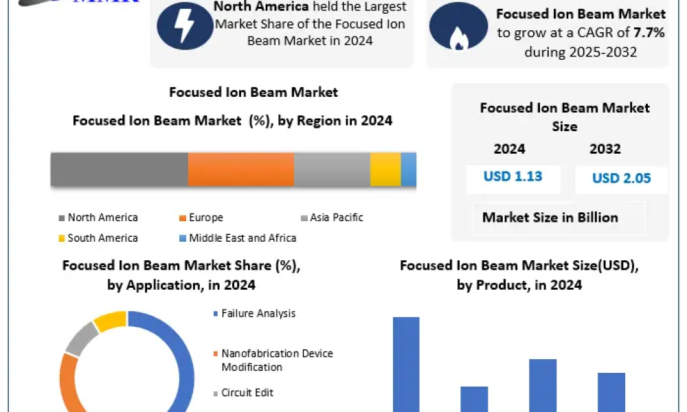
Focused Ion Beam (FIB) Market, valued at USD 1.13 billion in 2024, is forecasted to grow to USD 2.05 billion by 2032, registering a CAGR of 7.7%. Advancements in semiconductor manufacturing, failure analysis, and nanofabrication are fueling demand across various high-tech industries. North America dominates the market with a 34.7% revenue share in 2024, propelled by rapid growth in semiconductor R&D, advanced manufacturing capabilities, and robust governmental support.
Key Highlights & Insights
- Market Size & Growth: The FIB market size is projected to grow from USD 1.55 billion in 2024 to USD 2.36 billion by 2030 at a CAGR of 7.3%.
- Dominating Region: North America leads with 34.7% share, driven by strong semiconductor industry presence, cutting-edge research institutions, and investments in next-generation chip fabrication technologies.
- Leading Segment: Gallium (Ga+) liquid metal ion source dominates with 80.6% market share owing to its high precision and widespread adoption for semiconductor failure analysis and nanofabrication.
- Key Driver: Increasing complexity of semiconductor devices requiring precise defect analysis, coupled with rising nanotechnology research activities, are major growth factors.
Recent Developments
- 2024-2025: Thermo Fisher Scientific expanded its FIB-SEM product line offering enhanced precision and automation targeting semiconductor and materials science sectors.
- Hitachi High-Technologies launched advanced dual-beam FIB systems optimized for 3D nanostructure fabrication and analysis.
- JEOL Ltd. introduced new gas field ion sources (GFIS) enhancing resolution capabilities for life science and materials research.
- Several key players invested in AI-assisted defect detection and automated FIB systems to increase throughput and reduce operation complexity.
Market Dynamics
Growth Drivers:
- Rising demand for in-depth failure analysis of semiconductor components amid the intensifying chip manufacturing complexity.
- Expansion of nanofabrication and material science research requiring ultra-high spatial resolution imaging and milling.
- Increasing application of FIB technology in life sciences including biological sample preparation and 3D tomography.
- Adoption of AI and automation in FIB systems improves accuracy and operational efficiencies.
Challenges:
- High capital expenditure and maintenance costs restricting access to smaller laboratories.
- Requirement of skilled operators and extensive training for optimized FIB utilization.
- Material supply constraints for specialized ion sources and advanced manufacturing components.
Grab your free sample copy of this report today: https://www.maximizemarketresearch.com/request-sample/12057/
Regional Analysis
- North America: Largest and most mature market led by a dominant semiconductor ecosystem in the U.S. and Canada, encompassing key manufacturers, R&D hubs, and substantial government funding.
- Asia Pacific: Fastest-growing region supported by expanding semiconductor fabrication facilities in China, South Korea, Japan, and Taiwan, alongside growing research investments.
- Europe: Significant market with focus on research institutions and high-precision materials science applications.
- Rest of World: Emerging adoption driven by investments in nanotechnology and industrial applications.
Product Segmentation
- By Ion Source: Gallium (Ga+) Liquid Metal, Gas Field Ion Source (GFIS), Plasma Ion Source.
- By Application: Failure Analysis (largest segment), Nanofabrication, Device Modification, Circuit Edit.
- By End-Use Industry: Semiconductor & Electronics (largest), Material Science, Biosciences, Industrial Applications.
Key Trends
- Integration of AI and machine learning for automated defect detection and milling in FIB systems.
- Development of gas field and plasma ion sources for specialized applications requiring ultra-high-resolution and high-throughput processing.
- Growth in combined FIB-SEM systems that enable simultaneous imaging and etching for in-situ analysis.
- Expansion of applications into biological sciences for advanced imaging and sample preparation.
Quote
“North America’s leadership in the focused ion beam market is driven by a convergence of semiconductor innovation, robust research infrastructure, and rapid adoption of advanced microscopy techniques. As device geometries shrink and material complexities rise, FIB technology is becoming indispensable for precision manufacturing and scientific discovery.”
Focused ion beam technology is at the forefront of precision material modification and analysis, empowering semiconductors, nanotechnology, and life sciences sectors with unparalleled capabilities. With continued technological innovation and expanding applications, the global FIB market is set for sustained growth and transformative impact across diverse scientific and industrial domains.
About Maximize Market Research:
Maximize Market Research is one of the fastest-growing market research and business consulting firms serving clients globally. Our revenue impact and focused growth-driven research initiatives make us a proud partner of majority of the Fortune 500 companies. We have a diversified portfolio and serve a variety of industries such as IT & telecom, chemical, food & beverage, aerospace & defense, healthcare and others.
Contact Maximize Market Research:
MAXIMIZE MARKET RESEARCH PVT. LTD.
⮝ 3rd Floor, Navale IT park Phase 2,
Pune Banglore Highway, Narhe
Pune, Maharashtra 411041, India.
✆ +91 9607365656
🖂 [email protected]