
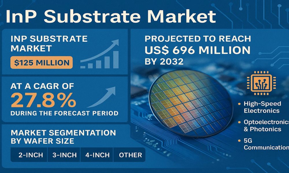
InP Substrate Market was valued at 125 million in 2024 and is projected to reach US$ 696 million by 2032, at a CAGR of 27.8% during the forecast period.
An InP (Indium Phosphide) substrate is a semiconductor wafer composed of indium phosphide material, prized for its superior electron mobility and high light emission efficiency. These substrates are critical components in high-speed electronics, optoelectronics, and photonics applications, particularly in 5G communications, data centers, and advanced sensor technologies. The market is segmented by wafer size, including 2-inch, 3-inch, 4-inch, 6-inch, and other diameters, with the 2-inch segment showing notable growth potential.
The market expansion is driven by increasing demand for high-performance semiconductors in telecommunication and defense sectors, coupled with advancements in compound semiconductor technologies. North America and Asia-Pacific dominate the market share, with the U.S. and China being key revenue contributors. Leading manufacturers such as Sumitomo Electric and AXT hold significant market positions, leveraging technological innovations to meet growing industry demands.
Access Your Free Sample Report Now- https://semiconductorinsight.com/download-sample-report/?product_id=117735
MARKET DYNAMICS
MARKET DRIVERS
Expanding 5G and Optical Communication Infrastructure to Boost Demand for InP Substrates
The global rollout of 5G networks and the continuous expansion of optical communication systems form a key driver for the InP substrates market. Indium Phosphide (InP) substrates are preferred for high-frequency applications due to their superior electron mobility and thermal stability. With 5G infrastructure demanding high-speed data transmission capabilities, the adoption of InP-based RF devices such as power amplifiers and switches has surged. Similarly, in fiber optic communication networks, InP substrates are critical components for laser diodes and photodetectors, enhancing bandwidth and efficiency. The anticipated increase in data traffic volumes due to IoT implementations and cloud computing further reinforces this demand trajectory.
Growth in Photonics and Optoelectronics Applications to Accelerate Market Expansion
Photonics and optoelectronics sectors are witnessing substantial R&D investments, contributing to the growing adoption of InP substrates. These substrates enable high-performance semiconductor lasers, LEDs, and sensors essential for applications ranging from medical imaging to autonomous vehicles. Notably, InP’s efficiency in converting electrical signals into light makes it indispensable for lidar systems—a technology critical for advanced driver-assistance systems (ADAS) and robotic automation. Furthermore, governmental initiatives supporting photonics research, such as those in Europe and North America, have accelerated commercialization, reinforcing market growth for InP substrates globally.
Increasing Demand for High-Speed Data Centers to Propel Market Growth
The exponential rise in hyperscale data centers, driven by cloud computing, AI, and big data analytics, is a significant factor compelling the need for InP substrates. These substrates enhance the efficiency of optical transceivers used in high-bandwidth interconnects, enabling faster data transfer rates while reducing power consumption—a critical requirement for sustainable data center operations. Investments in next-gen data centers, particularly in North America and Asia-Pacific, highlight the growing reliance on InP-based solutions to meet evolving technological demands.
Recent Development in the InP Substrate Market
- IQE plc Expands InP Substrate Production: IQE, a leading supplier of advanced semiconductor materials, announced the expansion of its indium phosphide (InP) substrate manufacturing capacity to meet rising demand from the data center, telecom, and photonics industries. The expansion includes investment in high-purity crystal growth and wafering technologies, aimed at supporting next-generation optical communication and 5G infrastructure.
- Sumitomo Electric Advances High-Quality InP Substrates: Sumitomo Electric introduced a new series of semi-insulating InP substrates with improved defect density control and enhanced thermal stability. These substrates are designed for high-speed photonic devices and 6G R&D applications.
- AXT Inc. Enhances Vertical Integration for InP Wafer Supply: AXT announced progress in its vertical integration strategy by securing raw material supply partnerships for indium. This move strengthens its position in the InP substrate market and ensures consistent wafer quality for photonics and sensing devices.
- Collaboration for Quantum Applications: A consortium of research institutes and companies in Europe launched a joint project to develop quantum photonics devices based on InP substrates. This development highlights the growing importance of InP in quantum computing and secure communications.
MARKET OPPORTUNITIES
Advancements in Quantum Computing to Unlock New Growth Avenues
Quantum computing represents a transformative opportunity for InP substrates, which are integral to developing qubit technologies and photonic quantum circuits. Their ability to operate at telecom wavelengths aligns with quantum communication needs, positioning InP as a strategic material for next-gen quantum devices. With governments and tech giants investing heavily in quantum R&D, collaborations between semiconductor manufacturers and research institutions could accelerate commercialization efforts in this niche.
Rising Demand for Satellite Communication Systems to Drive Future Adoption
The surge in low-earth orbit (LEO) satellite deployments for global broadband coverage underscores opportunities for InP-based RF components. These substrates enable high-efficiency power amplifiers and transceivers capable of operating in extreme conditions—a prerequisite for satellite communications. As private and public sectors expand satellite constellations, InP substrates are poised to play a vital role in meeting the technical demands of this high-growth sector.
List of Key InP Substrate Manufacturers
- Sumitomo Electric Industries (Japan)
- JX Advanced Metals Corporation (Japan)
- Beijing Tongmei Xtal Technology (AXT) (China/US)
- Zhuhai Dingtai Xinyuan (China)
- FanMei Strategic Metal Resources (China)
- Guangdong Tianding Sike New Materials (China)
- Yunnan Xinyao Semiconductor Materials (China)
Looking ahead, competition is expected to intensify as demand grows for larger diameter substrates (6-inch and above) and higher quality specifications. Companies with strong intellectual property portfolios in crystal growth technologies and the ability to scale production efficiently will likely gain market share in this high-growth semiconductor material segment.
Access Your Free Sample Report Now- https://semiconductorinsight.com/download-sample-report/?product_id=117735
Segment Analysis:
By Type
6-Inch Substrates Dominates the Market Due to High Demand in High-Performance Applications
The market is segmented based on type into:
- 2 inches
- 3 inches
- 4 inches
- 6 inches
- Other
By Application
Optical Module Devices Segment Leads Due to Expanding Fiber Optic Networks and Data Communication Needs
The market is segmented based on application into:
- Optical Module Devices
- RF Devices
- Sensor Devices
- Other Applications
By End-Use Industry
Telecommunications Segment Leads with Accelerating 5G Implementation
The market is segmented based on end-use industry into:
- Telecommunications
- Aerospace & Defense
- Healthcare
- Consumer Electronics
- Industrial
Other Topic- Passive Wireless Temperature Sensor Market
CONTACT US:
City vista, 203A, Fountain Road, Ashoka Nagar, Kharadi, Pune, Maharashtra 411014
[+91 8087992013]