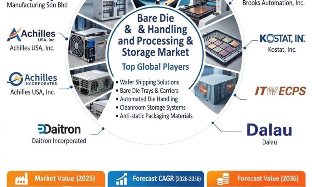
The global Bare Die Shipping & Handling and Processing & Storage Market reached USD 1.5 billion in 2025 and is projected to increase from USD 1.6 billion in 2026 to USD 3.2 billion by 2036, expanding at a 7.2% CAGR during the 2026–2036 forecast period. Market expansion is being supported by semiconductor assembly, advanced packaging, automation, and growing requirements for electrostatic discharge (ESD) and contamination control. SEMI projects semiconductor assembly and packaging equipment sales to rise 9.6% to USD 6.7 billion in 2026, following 20.8% growth in 2025.
Get detailed market forecasts, competitive benchmarking, and pricing trends: https://www.factmr.com/connectus/sample?flag=S&rep_id=10733
Global Segment Leaders
- Bare Die Handling Systems — 68.4% share in 2026: Leads the Product segment because exposed dies require controlled pickup, transfer, and retention before final packaging.
- Semiconductor Manufacturing — 41.9% share in 2026: Leads the Application segment as dies move through inspection, testing, temporary storage, and assembly processes.
- Semiconductor Foundries — 77.2% share in 2026: Leads the End Use segment due to high wafer throughput and increasing advanced packaging activity.
- Automated Die Handling Technology — 57.3% share in 2026: Leads the Technology segment because automated transfer supports precision and repeatability at production scale.
- Integrated Handling Platforms — 63.8% share in 2026: Leads the Formulation segment as manufacturers combine handling hardware with control systems, identification, and traceability.
- Direct Semiconductor Sales — 45.6% share in 2026: Leads the Distribution Channel segment because handling products often require technical qualification against semiconductor manufacturing and automation specifications.
Country-Level Performance
| Country | CAGR, 2026–2036 | Key Growth Driver |
| USA | 7.8% | In July 2026, the U.S. Department of Commerce announced support for expansion of silicon carbide semiconductor production in California, including new cleanroom space and manufacturing capacity. |
| South Korea | 7.2% | SEMI reported that semiconductor equipment spending in Korea is being supported by HBM investment, increasing handling requirements for vertically integrated die structures. |
| Germany | 6.8% | The ESMC open foundry in Dresden is expected to reach 480,000 wafers annually by 2029, while Infineon’s designated facility supports power and analog or mixed-signal semiconductor production. |
| Japan | 6.7% | Government policy in 2026 continued to emphasize stronger domestic semiconductor manufacturing sites and supply-chain resilience; SEMI projected Japanese semiconductor manufacturing capacity at approximately 4.7 million wafers per month in 2025. |
| UK | 6.5% | A semiconductor facility opened at the University of Southampton in 2025 with electron-beam lithography capability and access to an academic cleanroom. |
| France | 6.2% | The STMicroelectronics and GlobalFoundries project at Crolles is planned around 300 mm semiconductor production and is expected to reach approximately 620,000 wafers annually at full capacity. |
| Italy | 6.1% | In March 2026, the Ministry of Enterprises and Made in Italy signed a development agreement for the Silicon Box project in Novara, focused on back-end processing, advanced packaging, and testing. |
Regional Context
The USA and South Korea represent the faster-growing country markets in the report, with CAGRs of 7.8% and 7.2%, respectively. In the USA, semiconductor fabrication and advanced packaging investments are expanding domestic die-processing workflows. South Korea’s growth is linked closely to memory manufacturing and HBM applications, where multi-die structures increase the need for controlled handling.
Germany and Japan represent established semiconductor manufacturing bases with continued capacity expansion and supply-chain investment. Germany’s Dresden projects support automotive and industrial semiconductor production, while Japan is strengthening domestic semiconductor production infrastructure and supply-chain resilience.
The UK, France, and Italy show comparatively lower forecast CAGRs within the profiled countries. The UK is focused more on specialist semiconductor research and compound-semiconductor activity, while France is adding 300 mm production capacity at Crolles. Italy is increasing its role in semiconductor back-end processing through advanced packaging and chiplet-focused investment.
The full report covers North America, Latin America, Europe, East Asia, South Asia and Pacific, and the Middle East and Africa, with seven specifically profiled countries: the USA, UK, France, Germany, Italy, South Korea, and Japan.
Competitive Landscape
Key companies profiled in the Bare Die Shipping & Handling and Processing & Storage Market include Entegris, Inc.; 3M Company; Brooks Automation, Inc.; Kostat, Inc.; ITW ECPS; Dalau; Daitron Incorporated; Achilles USA, Inc.; and TT Engineering & Manufacturing Sdn Bhd. Entegris participates through bare die tray systems designed for device retention and compatibility with manual and automated handling. 3M competes through semiconductor carrier materials and ESD-protective packaging formats, while Brooks Automation provides semiconductor automation systems supporting material transfer and identification.
Recent developments cited in the report include the March 2026 development agreement between the Ministry of Enterprises and Made in Italy and Silicon Box for its Novara project, focused on back-end processing, advanced packaging, and testing. In July 2026, the U.S. Department of Commerce announced support for expansion of silicon carbide semiconductor production in California, including additional cleanroom space and manufacturing capacity.
Top Trending Reports:
About Fact MR
(Fact MR) is a leading provider of market research and consulting services, offering syndicated and customized research across industries including semiconductor manufacturing, advanced packaging, and electronics assembly.