
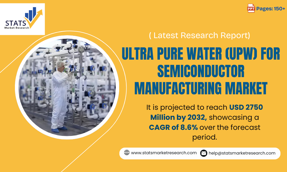
Global Ultra Pure Water (UPW) for Semiconductor Manufacturing Market to Reach USD 2.75B by 2032, Growing at 8.6% CAGR
Definition
Ultra Pure Water (UPW) refers to a highly specialized water grade used in semiconductor manufacturing where virtually all impurities are removed. UPW achieves resistivity levels exceeding 18.2 MΩ·cm and contaminant concentrations measured in parts per trillion. Achieving this level of purity requires a multi-stage purification process, including reverse osmosis, electrodeionization, advanced filtration, UV oxidation, and continuous monitoring systems.
In semiconductor fabs, UPW is mission-critical infrastructure, directly affecting wafer yields, defect rates, and overall production efficiency. As nodes shrink below 7nm, purity standards become increasingly stringent. UPW is used in wafer cleaning, chemical mechanical planarization (CMP), etching, stripping, backgrind, and lithography processes, making it indispensable for leading-edge semiconductor manufacturing.
The market for UPW is dominated by highly specialized suppliers, with Japanese companies like Kurita, Organo, and Nomura Micro Science collectively controlling over 80% of installations globally. This reflects both the technical complexity and the capital-intensive nature of UPW systems.
Recent Developments in the Ultra Pure Water (UPW) for Semiconductor Manufacturing Market
Recent developments in the UPW for semiconductor manufacturing market are heavily focused on sustainability, efficiency, and meeting increasingly stringent purity requirements. As semiconductor fabrication plants (fabs) consume massive amounts of water, a key trend is the development of advanced water recycling and reclamation technologies. Manufacturers are implementing closed-loop systems and integrating technologies like counter-flow reverse osmosis to dramatically reduce their reliance on freshwater sources. Additionally, the drive for smaller, more advanced chips is pushing the boundaries of water purity, with fabs now requiring contaminant levels to be measured in parts-per-quadrillion. To achieve this, there is a growing adoption of advanced purification methods such as fractional electrodeionization and specialized filtration membranes that can remove difficult contaminants like boron and silica, which can compromise chip yield. The use of AI and real-time monitoring is also becoming more prevalent to optimize water usage, reduce waste, and ensure consistent quality throughout the entire manufacturing process.
Major Distribution Channels
The distribution of Ultra Pure Water in the semiconductor industry is unique as it is not a “product” that is simply sold and shipped. Instead, it is a service-based market where companies specialize in the design, construction, and operation of on-site UPW plants. The primary distribution channel is a direct, long-term relationship between specialized water treatment companies and semiconductor manufacturers. These water treatment providers, such as Veolia, Evoqua Water Technologies, and Kurita Water Industries, are essentially hired to build and manage the entire UPW infrastructure within a fab. They are responsible for the entire process, from treating raw municipal water to providing the final UPW at the point of use. This model is preferred because of the highly technical nature and immense scale required to produce and maintain UPW. Another, though less common, channel involves equipment manufacturers selling individual components like membranes, pumps, and purification systems to semiconductor companies that choose to manage their own UPW production in-house.
Market Size
Global Ultra Pure Water (UPW) for Semiconductor Manufacturing market was valued at USD 1568 million in 2024 and is projected to grow to USD 2750 million by 2032, registering a CAGR of 8.6%.
- 2024: USD 1568 million
- 2025: USD 1700 million
- 2032: USD 2750 million
The growth is driven by:
- Increasing semiconductor fabrication activities worldwide, especially in Asia-Pacific.
- Transition to advanced process nodes (<7nm) requiring extreme water purity.
- Expansion of fabrication facilities (fabs) with capacities exceeding 2,000–5,000 m³/day of UPW.
- Investments under U.S. CHIPS Act, EU Chips Act, and domestic semiconductor incentives, which demand localized and advanced UPW infrastructure.
Historically, the market has grown steadily as semiconductor fabs increased production capacities. Advanced nodes, EUV lithography adoption, and 3D NAND architectures have all contributed to a rising demand for UPW systems with higher TOC control (<1 ppb) and particle counts <5 particles/mL at 0.05μm.
Download FREE Sample of this Report @ https://www.statsmarketresearch.com/download-free-sample/8058709/global-ultra-pure-water-for-semiconductor-manufacturing-forecast-market
Market Dynamics
Market Drivers
- Rising Semiconductor Production Capacity: The global semiconductor industry is investing over $500 billion between 2021-2025 to expand fabrication capacity. Each new fab requires sophisticated UPW systems to maintain wafer yield and process integrity.
- Stringent Purity Requirements in Advanced Nodes: Sub-5nm semiconductor nodes demand ultra-low TOC and particle levels, making UPW systems indispensable. UPW quality impacts 30-40% of yield parameters, incentivizing continuous infrastructure upgrades.
- Geopolitical Reshoring Initiatives: Policies such as the U.S. CHIPS Act ($52 billion incentives) and EU Chips Act are stimulating domestic semiconductor manufacturing, driving demand for localized UPW systems.
- Sustainability Initiatives: Water recycling and recovery systems are increasingly important in water-stressed regions. Next-generation UPW systems achieve 85–95% water recovery, aligning with environmental regulations and sustainability goals.
Market Restraints
- High Capital & Operational Costs: UPW systems are 5–7% of total fab costs, with multi-stage purification and maintenance costing $3–5 million annually per system. This limits adoption among smaller fabs and developing markets.
- Technical Complexity: Advanced nodes (<3nm) require contamination control at parts-per-quadrillion levels, necessitating real-time monitoring systems ($1–2 million per fab). Transition to new materials like cobalt and ruthenium also introduces additional purification challenges.
- Energy Intensity: UPW generation consumes 3–5 kWh/m³, up to 10x more than conventional water treatment, creating sustainability and cost pressures for fabs pursuing net-zero goals.
Market Opportunities
- Smart UPW Monitoring: Integration of IoT sensors and AI analytics reduces contamination incidents by 40–60% and predictive maintenance cuts downtime by 30%. Cloud-based platforms allow fab-wide visibility across 200+ water parameters.
- Circular Water Economy Models: Systems with 95%+ water recovery reduce water procurement costs by 25–35%, enhancing sustainability in drought-prone regions. Blockchain-based water management programs improve both environmental credentials and supply chain resilience.
- Packaged UPW Solutions: Modular systems for compound semiconductors (GaN, SiC) and advanced packaging allow 100–500 m³/h capacity, enabling faster deployment and 30–40% lower upfront costs for specialty fabs and R&D centers.
Market Challenges
- Supply Chain & Equipment Shortages: The highly specialized nature of UPW components leads to long lead times and high reliance on few suppliers, especially for advanced membranes and sensors.
- Rising Competition from Regional Suppliers: Chinese and Taiwanese manufacturers are increasing production while upgrading technologies, creating price-based competition.
- Maintenance & Operational Expertise: Running multi-stage UPW systems requires trained personnel, increasing labor costs and operational risk.
Segment Analysis
By Type
- Below 100 m³/h
- 100–500 m³/h – Dominates due to high demand in mid-scale semiconductor fabs
- 500–1000 m³/h
- Others
By Application
- Wafer Cleaning – Leads due to critical role in wafer yield
- Etching
- Stripping
- CMP (Chemical Mechanical Planarization)
- Backgrind
- Lithography
- Others
By Technology
- Reverse Osmosis – Holds major share due to high purification efficiency
- Ion Exchange
- Electrodeionization
- UV Oxidation
- Others
By End User
- Foundries – Lead due to large-scale production facilities
- IDMs (Integrated Device Manufacturers)
- OSATs (Outsourced Semiconductor Assembly & Test)
- R&D Facilities
Get the Complete Report & TOC @ https://www.statsmarketresearch.com/global-ultra-pure-water-for-semiconductor-manufacturing-forecast-market-8058709
Regional Analysis
- North America: Strong demand from U.S. fabs under the CHIPS Act; focus on water recycling and energy efficiency.
- Europe: Growing adoption in Germany, France, and the Netherlands, driven by advanced packaging and EU Chips Act incentives.
- Asia-Pacific: Fastest-growing region due to TSMC, SMIC, Samsung fabs, and high EUV adoption.
- Latin America & Middle East: Moderate growth with demand from emerging semiconductor hubs and R&D facilities.
Competitor Analysis
The UPW market is highly concentrated, with Japanese firms historically dominating. Key players focus on technology innovation, strategic expansion, and integrated solutions:
- Kurita Water Industries: Market leader with strong global UPW installations
- Organo Corporation: Advanced purification systems with SMART-UPW AI-based monitoring
- Nomura Micro Science: Specialized in high-end UPW for sub-5nm nodes
- Veolia Environment: Expanded via acquisitions in Asia
- Evoqua Water Technologies: Focus on modular and localized UPW solutions
- SKion Water GmbH: Germany-based solutions for European fabs
- Regional Chinese & Taiwanese players: Guangdong Tanggu Environmental Technology, Taiwan Pure Water Technology
Key Company
- Kurita Water Industries Ltd. (Japan)
- Organo Corporation (Japan)
- Nomura Micro Science Co., Ltd. (Japan)
- Veolia Environment S.A. (France)
- Evoqua Water Technologies (U.S.)
- SKion Water GmbH (Germany)
- Guangdong Tanggu Environmental Technology (China)
- Taiwan Pure Water Technology (Taiwan)
- Atlas High Purity Water (U.S.)
Geographic Segmentation
- North America: U.S., Canada, Mexico
- Europe: Germany, France, U.K., Netherlands, Rest of Europe
- Asia-Pacific: China, Taiwan, South Korea, Japan, Rest of APAC
- Latin America: Brazil, Argentina, Rest of LATAM
- Middle East & Africa: GCC Countries, South Africa, Rest of MEA
FAQs
Q1: What is the current market size of Ultra Pure Water (UPW) for Semiconductor Manufacturing?
A: The market was valued at USD 1568 million in 2024 and is projected to reach USD 2750 million by 2032.
Q2: Which are the key companies operating in this market?
A: Kurita, Organo, Nomura Micro Science, Veolia, Evoqua, SKion Water, Guangdong Tanggu, Taiwan Pure Water, Atlas High Purity Water are major players.
Q3: What are the key growth drivers?
A: Rising semiconductor fab capacity, sub-7nm node adoption, strict water purity standards, and sustainability initiatives.
Q4: Which regions dominate the market?
A: Asia-Pacific is the fastest-growing region, followed by North America and Europe.
Q5: What are the emerging trends?
A: Smart UPW monitoring, circular water economy models, modular UPW systems for compound semiconductors, and AI-driven predictive maintenance.
About Us
☎️ International: +1 (332) 2424 294
📄 Website: www.statsmarketresearch.com
Join us on LinkedIn:- https://www.linkedin.com/company/statsmarketresearch