
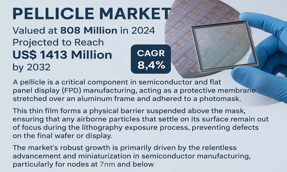
Pellicle Market was valued at 808 million in 2024 and is projected to reach US$ 1413 million by 2032, at a CAGR of 8.4% during the forecast period.
A pellicle is a critical component in semiconductor and flat panel display (FPD) manufacturing, acting as a protective membrane stretched over an aluminum frame and adhered to a photomask. This thin film forms a physical barrier suspended above the mask, ensuring that any airborne particles that settle on its surface remain out of focus during the lithography exposure process, thereby preventing defects on the final wafer or display. This technology is indispensable for maintaining high production yields and superior chip quality.
The market’s robust growth is primarily driven by the relentless advancement and miniaturization in semiconductor manufacturing, particularly for nodes at 7nm and below. The surge in demand for high-performance computing, artificial intelligence chips, and the expansion of the FPD industry further propels this growth. The market is highly consolidated, with the top three players—Mitsui Chemicals, Shin-Etsu, and FINE SEMITECH—commanding a collective revenue share of approximately 85.67% in 2023. Asia dominates the global landscape, accounting for the largest market share, fueled by massive semiconductor fabrication investments in China, Taiwan, and South Korea.
Receive Your Sample Report at No Cost- https://semiconductorinsight.com/download-sample-report/?product_id=117539
MARKET DYNAMICS
MARKET DRIVERS
Accelerated Semiconductor Miniaturization Driving Pellicle Demand
The relentless push toward semiconductor miniaturization represents the primary driver for pellicle market growth. As chip manufacturers transition to advanced nodes below 7nm, the requirement for defect-free photomasks becomes increasingly critical. The semiconductor industry’s migration to extreme ultraviolet lithography (EUVL) technology, which operates at 13.5nm wavelength, has created unprecedented demand for specialized pellicles capable of withstanding high-energy exposure while maintaining optical transparency. The global semiconductor equipment market, valued at over $100 billion annually, directly influences pellicle consumption patterns. With foundries investing approximately $20 billion annually in new fabrication facilities, the corresponding demand for photomasks and protective pellicles continues to escalate. This technological evolution necessitates pellicles with thickness variations controlled within 0.5nm and defect densities below 0.001 particles/cm², driving both technical innovation and market expansion.
Expanding Flat Panel Display Manufacturing Boosting Market Growth
The global display industry’s rapid expansion, particularly in organic light-emitting diode (OLED) and micro-LED technologies, represents another significant growth driver for the pellicle market. The flat panel display sector, which consumes approximately 25% of global pellicle production, requires increasingly sophisticated photomask protection as pixel densities approach 1000 pixels per inch. The transition to Generation 10.5 and larger display substrates, measuring 2940×3370mm, necessitates correspondingly larger pellicles with uniform optical properties across expanded surface areas. This scaling challenge has driven innovation in membrane materials and frame design, with leading manufacturers developing pellicles capable of maintaining <98% transmittance while providing effective particulate protection. The display industry’s compound annual growth rate of approximately 6-8% directly translates to increased pellicle consumption, particularly across Asian manufacturing hubs where over 85% of global display production occurs.
Furthermore, the integration of advanced lithography techniques in display manufacturing, including multi-patterning approaches, has increased photomask usage rates and consequently boosted pellicle replacement cycles. The average semiconductor fabrication facility utilizes between 5,000-10,000 photomasks simultaneously, each requiring periodic pellicle replacement every 12-18 months due to optical degradation and particulate accumulation.
➤ For instance, leading semiconductor manufacturers report that pellicle-related yield improvements can reduce wafer scrap rates by 2-3%, representing annual savings exceeding $50 million per high-volume fabrication facility.
Additionally, the emergence of advanced packaging technologies, including 2.5D and 3D integration schemes, has created new application segments for pellicles in back-end semiconductor processes, further expanding market opportunities beyond traditional front-end lithography applications.
Recent Developments in the Pellicle Market
- Advancements in Photomask Protection Technology
Manufacturers are developing next-generation pellicles with enhanced transmittance and durability to protect photomasks from contamination during high-volume semiconductor manufacturing. - Expansion of Semiconductor Manufacturing
With the growing adoption of advanced nodes (7nm, 5nm, and below), the demand for high-performance pellicles has surged, prompting companies to increase production capacities globally. - Introduction of EUV-Compatible Pellicles
Major players have launched pellicles compatible with Extreme Ultraviolet (EUV) lithography, which is essential for next-gen chip fabrication, offering better defect protection and higher yield rates. - Strategic Collaborations and Partnerships
Key manufacturers are entering collaborations with semiconductor fabs to co-develop customized pellicle solutions, improving product performance and addressing specific lithography challenges. - Focus on Sustainability and Material Innovation
Companies are exploring eco-friendly and more resilient materials for pellicles, aiming to reduce waste and increase lifecycle efficiency in semiconductor production.
MARKET OPPORTUNITIES
Emerging Applications in Advanced Packaging and Heterogeneous Integration Creating New Growth Frontiers
The rapid evolution of advanced packaging technologies presents substantial growth opportunities for the pellicle market. The adoption of fan-out wafer-level packaging (FOWLP), 2.5D interposers, and 3D integration schemes requires sophisticated lithography processes that utilize photomasks protected by specialized pellicles. The advanced packaging market, growing at approximately 8% annually, represents a potential addressable market expansion of $120-150 million for pellicle manufacturers. Particularly promising is the development of tailored pellicle solutions for through-silicon via (TSV) formation and redistribution layer patterning, where unique material requirements and process conditions create opportunities for product differentiation. The integration of compound semiconductors and photonic devices with silicon substrates further expands application possibilities, requiring pellicles optimized for non-standard wavelengths and exposure conditions.
Additionally, the emergence of quantum computing and neuromorphic computing architectures creates new opportunities for specialized pellicle applications. These emerging technologies utilize unconventional lithography approaches that often operate at non-standard wavelengths or require unique mask protection schemes. The development of pellicles capable of supporting these novel lithography methods represents a potential growth segment that could account for 5-7% of market revenue by 2030. The increasing adoption of multi-beam mask writers and other advanced mask fabrication technologies also drives demand for corresponding pellicle innovations, particularly in the area of defect inspection and metrology compatibility.
Moreover, the ongoing expansion of semiconductor manufacturing capacity globally, particularly in North America and Europe following recent semiconductor independence initiatives, creates substantial opportunities for market geographic diversification. The commitment of over $200 billion in new semiconductor fabrication investment outside traditional Asian manufacturing hubs will necessitate local pellicle supply chains, reducing logistics costs and improving supply security for end-users while creating new market access opportunities for manufacturers.
List of Key Pellicle Manufacturing Companies Profiled
- MITSUI Chemicals, Inc. (Japan)
- Shin-Etsu Chemical Co., Ltd. (Japan)
- FINE SEMITECH Corporation (South Korea)
- Micro Lithography, Inc. (MLI) (U.S.)
- S&S Tech Co., Ltd. (South Korea)
- INKO Engineering Corporation (South Korea)
- NEPCO (Japan)
- Canatu Oy (Finland)
Receive Your Sample Report at No Cost- https://semiconductorinsight.com/download-sample-report/?product_id=117539
Segment Analysis:
By Type
Pellicle for Quartz Mask Segment Dominates the Market Due to its Critical Role in Advanced Semiconductor Lithography
The market is segmented based on type into:
- Pellicle for Quartz Mask
- Pellicle for Soda Mask
- EUV Pellicle
- Others
By Application
Semiconductor Segment Leads Due to High Adoption in Chip Manufacturing and Miniaturization Trends
The market is segmented based on application into:
- Semiconductor
- Flat Panel Display (FPD)
- Photovoltaics
- Others
By Material
Polymer-based Pellicles Hold Significant Market Share Due to Their Optical Properties and Cost-effectiveness
The market is segmented based on material into:
- Polymer-based Pellicles
- Silicon-based Pellicles
- Nitride-based Pellicles
- Others
By Technology Node
Sub-10nm Technology Node Segment Experiences Rapid Growth Driven by Advanced Chip Fabrication Requirements
The market is segmented based on technology node into:
- Above 28nm
- 10nm-28nm
- 7nm-10nm
- Below 7nm
Other Topic- Generator Circuit Breaker (GCB) Market
CONTACT US:
City vista, 203A, Fountain Road, Ashoka Nagar, Kharadi, Pune, Maharashtra 411014
[+91 8087992013]