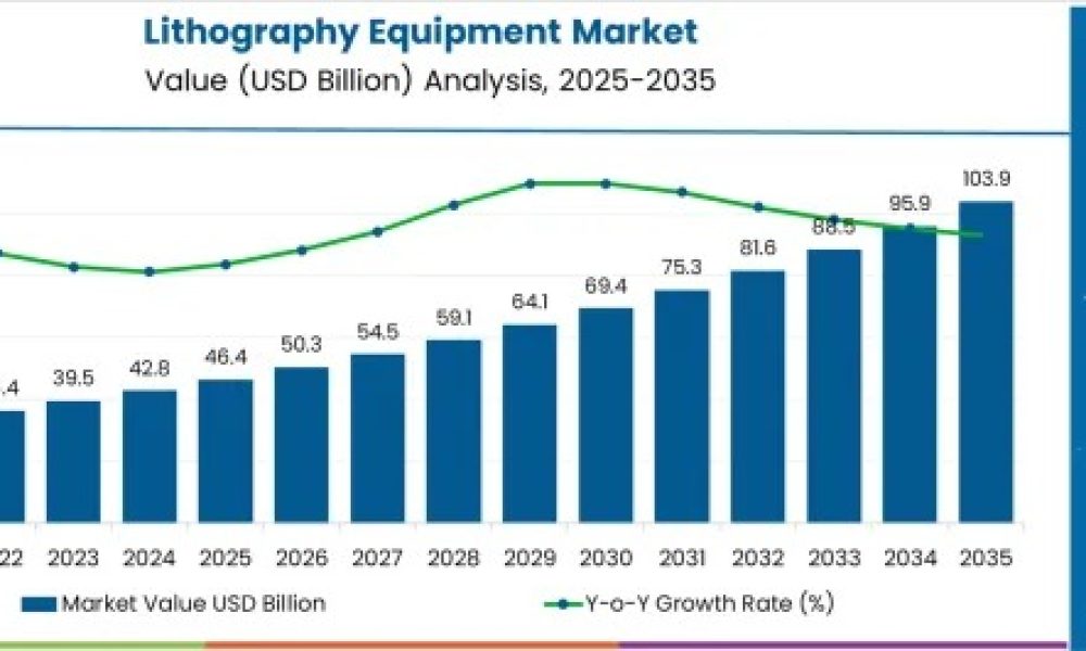
The global lithography equipment market is on track to grow from USD 46.4 billion in 2025 to approximately USD 103.9 billion by 2035, expanding at a robust CAGR of 8.4%. This growth underscores the industry’s vital role in powering the semiconductor revolution and next-generation chip manufacturing worldwide.
During the early adoption phase (2020–2024), the market grew gradually from USD 31.0 billion to USD 46.4 billion as semiconductor manufacturers began integrating advanced lithography systems for high-precision chip fabrication. With production lines scaling and standardization across fabrication plants, the market enters its rapid expansion phase (2025–2030) before consolidating into a mature landscape by 2035.
Request For Sample Report | Customize Report | Purchase Full Report –
EUV Technology Leads the Transformation
Extreme Ultraviolet (EUV) Lithography is projected to capture 42.6% of market revenue in 2025, enabling sub-10nm patterning for advanced chips. EUV reduces defects, boosts efficiency, and supports next-gen processors, positioning it as a critical tool in semiconductor manufacturing.
Key Points:
- Dominant segment with high precision and scalability
- Supports high-density memory and next-gen processors
- ASML drives innovations in optics, power, and throughput
Optical Lithography Remains a Workhorse
Optical/Photolithography holds 47.9% revenue share in 2025 due to cost-effectiveness and reliability. It supports multi-patterning and legacy nodes, ensuring continued relevance in high-volume fabs and maintaining a strong presence in mature semiconductor production.
Key Points:
- Largest revenue share in 2025
- Reliable, adaptable, and cost-effective
- SCREEN Holdings and SUSS MicroTec advance resolution and immersion technologies
Advanced Packaging Drives Market Demand
Advanced Packaging contributes 38.4% of market revenue in 2025. Technologies like 3D stacking, wafer-level packaging, and SiP increase demand for precision lithography, enabling miniaturized, high-performance devices across AI, 5G, automotive, and data center applications.
Key Points:
- Rising need for ultra-accurate patterning
- Supports miniaturization and energy-efficient devices
- Expands adoption across AI, 5G, and automotive electronics
Regional Growth Insights: Asia-Pacific at the Forefront
The Asia-Pacific region dominates the global lithography equipment landscape, fueled by robust semiconductor manufacturing ecosystems in China, Japan, South Korea, and Taiwan.
- China leads with a projected CAGR of 11.3%, supported by aggressive investments in domestic chip production and government-backed semiconductor programs.
- India, growing at 10.5% CAGR, benefits from national initiatives promoting electronics manufacturing and semiconductor self-reliance.
- In Europe, Germany (9.7%) and the UK (8.0%) sustain steady growth driven by strong R&D investment and automotive electronics.
- The United States, with 7.1% CAGR, remains a mature yet vital market focusing on innovation, automation, and fab modernization.
Market Dynamics: Precision, Reliability, and Integration
Resolution and throughput remain the key differentiators across regional markets. North America and Europe prioritize EUV and advanced DUV systems for sub-5nm node production, while Asia-Pacific emphasizes cost-effective mid-range tools for mass-market electronics.
Reliability and uptime are critical factors influencing purchasing decisions. Global fabs seek systems with predictive maintenance, remote diagnostics, and energy-efficient operation to ensure continuous production. Suppliers focusing on automation, integrated software compatibility, and low maintenance designs are gaining competitive advantage.
Get data that aligns with your strategic priorities — ask for report customization today:
Top Companies Shaping the Market
The photolithography and semiconductor equipment market is driven by global leaders and innovators, advancing EUV, immersion, nanoimprint, and MEMS technologies to meet growing semiconductor fabrication demands.
Key Market Players:
- ASML Holding N.V. – EUV leadership
- Nikon Corporation – Immersion lithography
- Canon Inc. – Immersion lithography
- Veeco Instruments Inc. – Wafer bonding, MEMS lithography
- SUSS MicroTec AG – MEMS lithography solutions
- EV Group – Advanced wafer bonding
- SCREEN Holdings Co., Ltd. – Lithography systems
- Onto Innovation Inc. – Inspection technologies
- JEOL Ltd. – Electron beam lithography
- Neutronix Quintel Inc. (NXQ) – Precision tools
- Advantest – Semiconductor testing solutions
- Shanghai Micro Electronics Equipment (Group) Co., Ltd. – Regional innovator
Future Outlook: Accelerating the Semiconductor Frontier
The lithography equipment market’s trajectory reflects the broader transformation of the global semiconductor ecosystem. As demand for AI chips, IoT devices, and advanced memory continues to surge, lithography remains the technological backbone enabling finer geometries and higher efficiency.
Rising capital expenditure on fabs, ongoing R&D in optical and electron-beam lithography, and government-backed manufacturing initiatives will further drive the market through 2035. The integration of AI-driven process control, automation, and metrology will define the next era of precision manufacturing.
Have a specific Requirements and Need Assistant on Report Pricing or Limited Budget please contact us – [email protected]
About Future Market Insights (FMI)
Future Market Insights, Inc. (FMI) is an ESOMAR-certified, ISO 9001:2015 market research and consulting organization, trusted by Fortune 500 clients and global enterprises. With operations in the U.S., UK, India, and Dubai, FMI provides data-backed insights and strategic intelligence across 30+ industries and 1200 markets worldwide.
Contact Us:
Future Market Insights Inc.
Christiana Corporate, 200 Continental Drive,
Suite 401, Newark, Delaware – 19713, USA
T: +1-347-918-3531